|
|
Quantum Optical and Photonic devices Research
|
Research Groups
Quantum Optical and Photonic devices Research Group
The world’s ever-increasing energy demands call for defining new schemes for efficient and sustainable power generation. Energy harvestion utilizing the solar spectrum is a topic of hot debate in today’s scientific community. In 1hr, the sun delivers enough energy to the earth to meet global needs for an entire year. According to a theoretical estimate, the world’s entire energy requirements can be met by utilizing the full length of the energy delivered on less than a tenth of the area of Sahara [Nature 2008; 454:816–23]. As time goes on, a variety of solar technologies will be combined to power entire communities and industries. Third Generation solar cells have the potential to overcome the Shockley-Queisser limit of 33% power conversion efficiency.
The key objective of our group is to set the grounds for the next generation pollution-free and highly efficient green power production. Quantum dots/wires/dyes/organic material sensitized photovoltaics are the current focus of research. We aim at engineering advanced materials and processes to develop efficient, sustainable and cost-effective schemes to overcome the country’s energy starvation issues.
In addition to that, Quantum Device Research Group is aimed at conducting experimentaland theoretical studies for semiconductor nano-crystlas within the quantum onfinement regime ,for optoelectronic applications including Light Emitting Diodes and solid state display technology which
Objectives
Below is the detail of the scientific objectives being probed:
- Structural evolution of the materials forming the cell electrodes and carrier transport layers for LED and solid state display device applications.
- Effect of morphological evolution of the materials used as an electrode layer on the overall device efficiency.
- Colloidal synthesis and characterization of sulphide based quantum dots as a sensitizer layer for solar cells and LEDs
- To look for novel materials to be used in energy conservation devices .
- Modeling and simulation of gaseous adsorption on materials for efficient energy harvestion.
- Theoretical investigation of the various quantum phenomena occurring at the device scale thus affecting the overall working.
- Increased light adsorption by the active region of the photovoltaic and LED devices .
- Increased light to power conversion efficiency in solar cells .
- Maximize the multiple carrier generation process in quantum dots .
- Increase the exciton lifetime for sustained current.
- Developing cost-effective energy and optical devices.
- Increasing luminous efficacy and charge carrier life time in inorganic semiconductor LEDs based on quantum dots.
- Shifting the emission spectrum of QLEDs towards red region for efficient light emission
- Growth of high density of uniformly ordered ZnS nanowires using a combination of block copolymer lithography and catalyst assisted growth via thermal evaporation.
- Tailoring the optical and electronic properties of ZnS nanowires for optical devices and detectors.
- Ensuring energy, environmental and economic security of the community at large.
Microscopy and Spectroscopy Lab
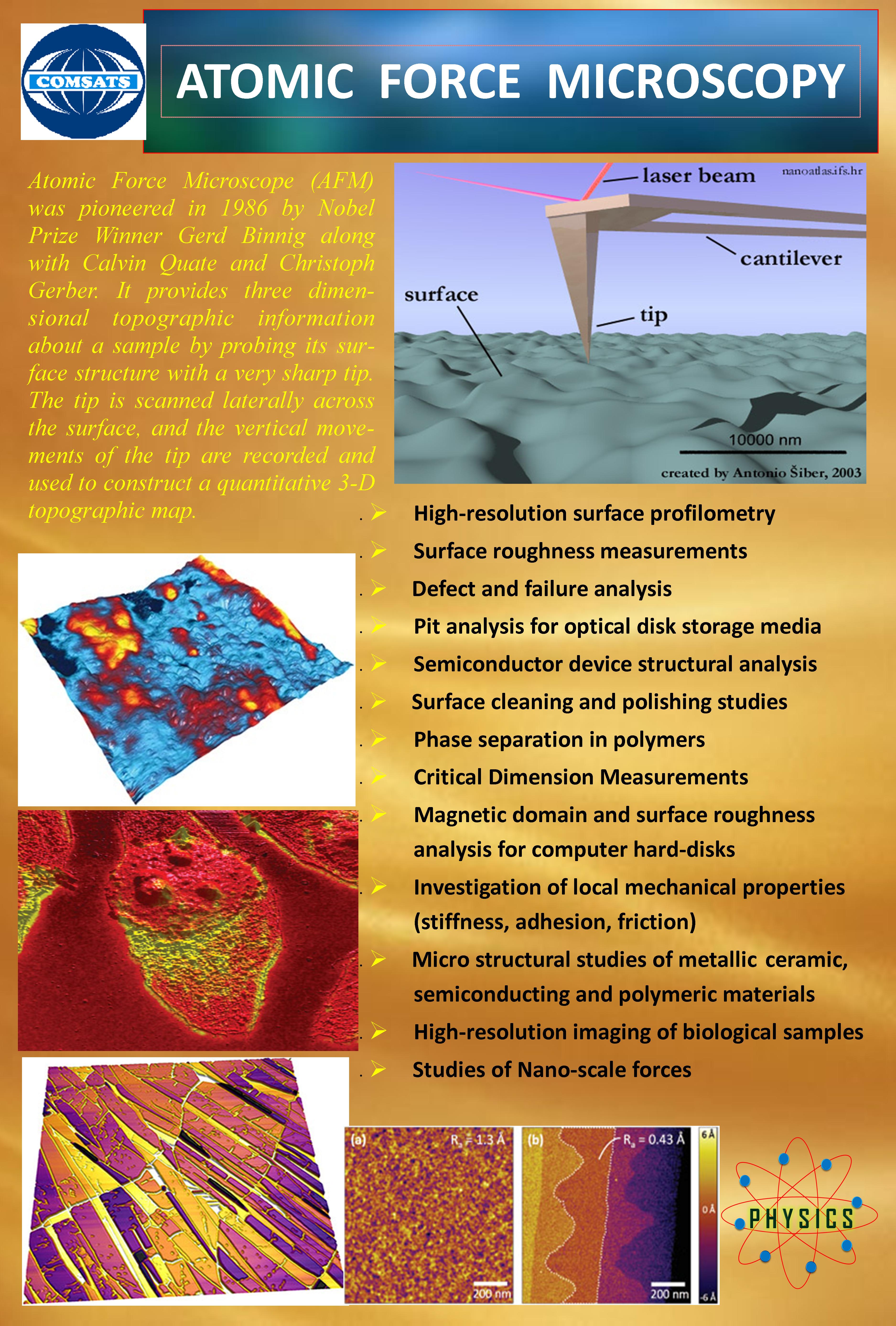
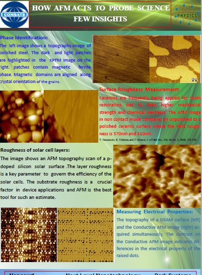
To do state of art science, we need state of art facilities. Such a facility has been developed at the Department of Physics which includes the advanced equipment to do the imaging as well as spectroscopic analysis. We are pleased to announce the successful installation of an Atomic Force Microscope to do nano-scale science. The AFM uses a two-dimentional flexure stage to scan the sample in the XY direction, and a stacked piezoelectric actuator to scan the probe cantilever in the Z direction only. This decoupled motion of z-scanner demonstrates high orthogonality and an excellent out-of-plane motion profile. The AFM not only includes all the basic imaging modes e.g. contact, non-contact and tapping mode but also gives the advantage to magnetic domain analysis, nano-indentation and electronic property analysis.
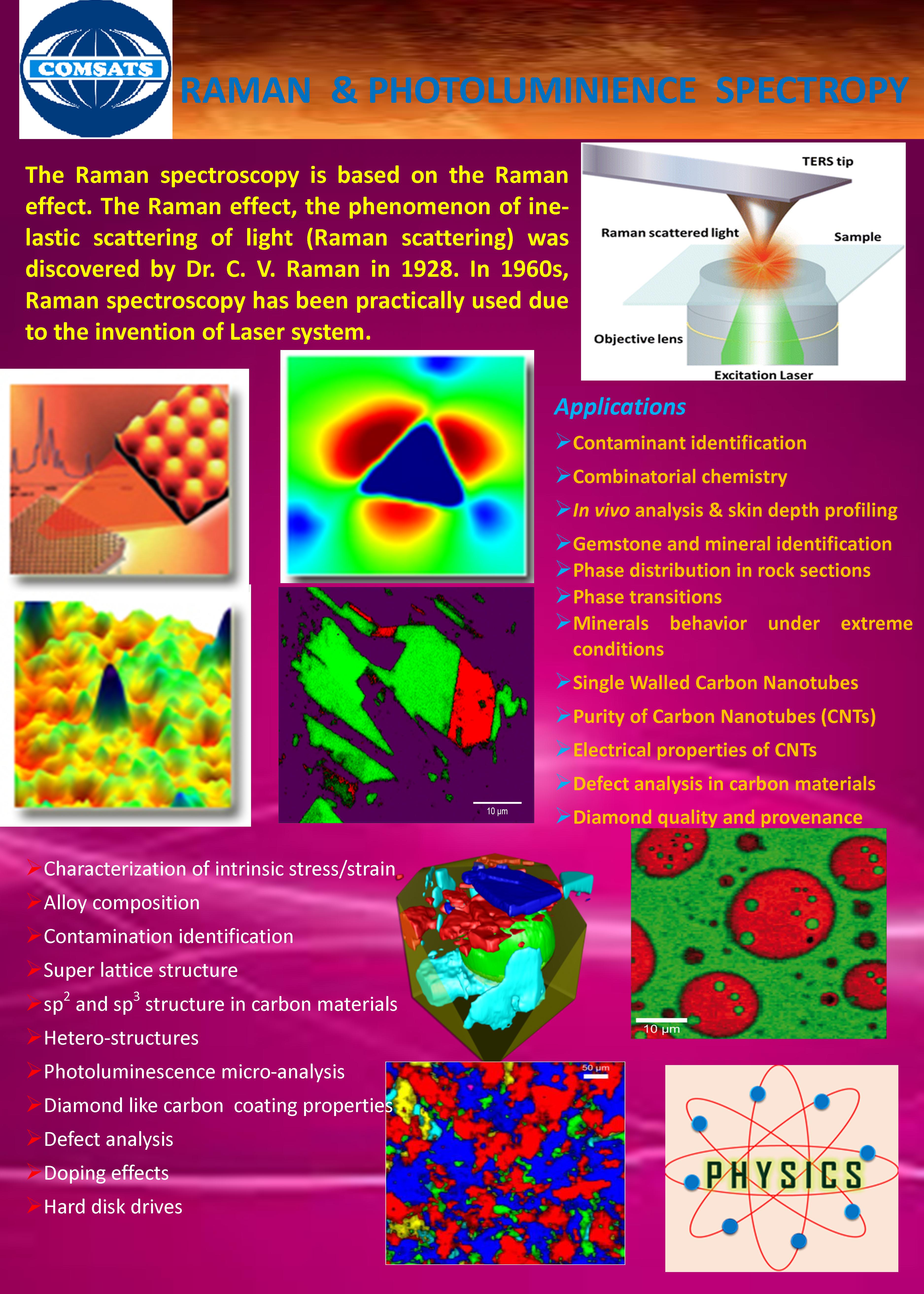
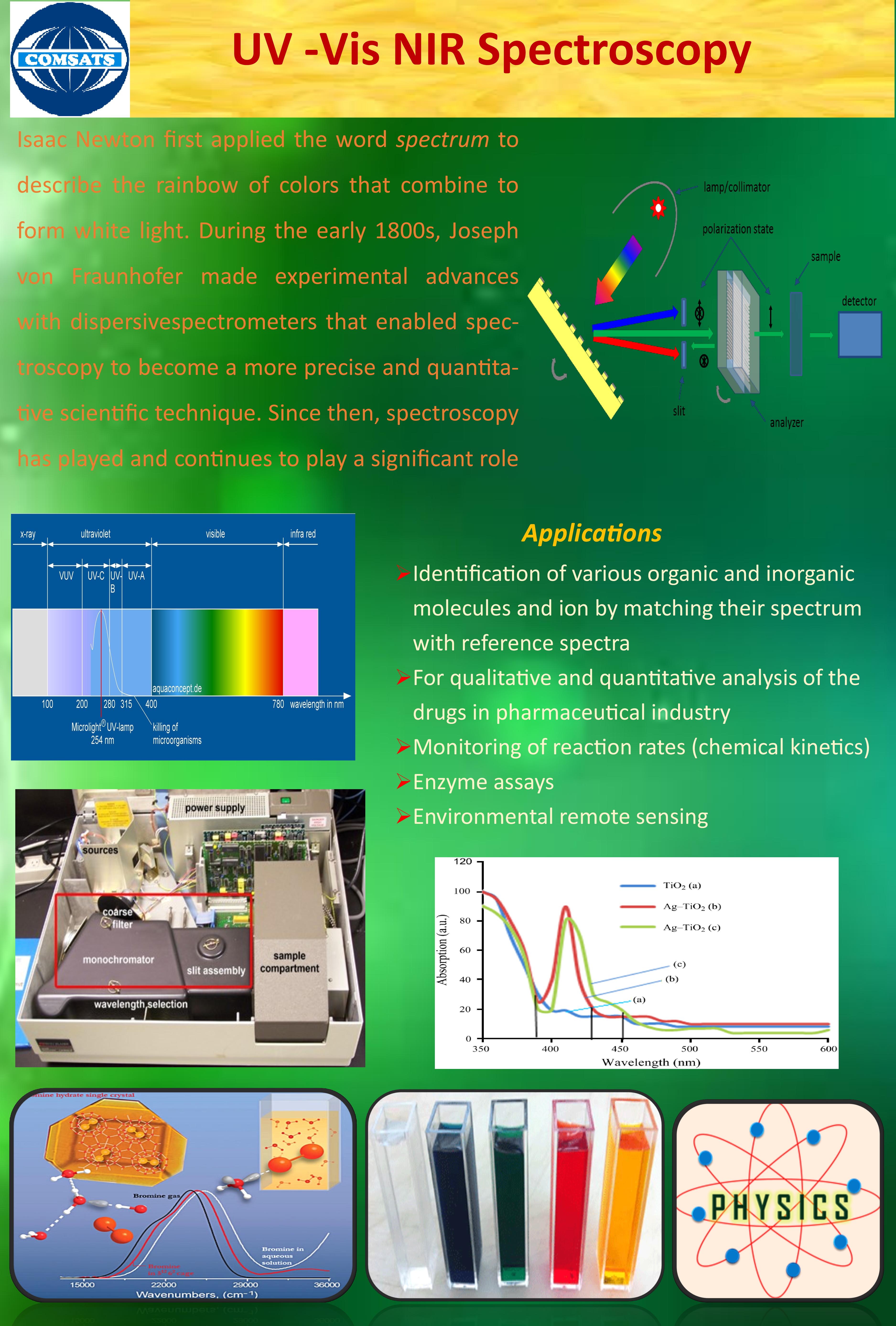
At the same time, the laboratory also includes the facility of inverted optical microscope to do live imaging with the magnification upto 100x. The area is soon to house a UV-VIS spectrometer and Raman/PL spectroscopy system to determine the optical characteristics of the grown structures. "
|
|